- 您现在的位置:买卖IC网 > Sheet目录505 > RTR025N05TL (Rohm Semiconductor)MOSFET N-CH 45V 2.5A TSMT3
RTR025N05
Data Sheet
350
300
250
200
I D = 2.5A
I D = 1.2A
Ta=25°C
Pulsed
1000
100
t d (off)
t f
Ta=25°C
V DD = 25V
V GS =4.5V
R G =10 ?
Pulsed
5
4
3
150
2
100
10
Ta=25°C
V DD = 25V
50
0
1
t r
t d (on)
1
0
I D = 2.5A
R G =10 ?
Pulsed
0
2
4
6
8
10
0.01
0.1
1
10
0
1
2
3
4
1000
100
10
GATE-SOURCE VOLTAGE : V GS [V]
Fig.10 Static Drain-Source On-State
Resistance vs. Gate Source Voltage
Ciss
Crss
Ta=25°C
Coss
f=1MHz
V GS =0V
DRAIN-CURRENT : I D [A]
Fig.11 Switching Characteristics
TOTAL GATE CHARGE : Qg [nC]
Fig.12 Dynamic Input Characteristics
0.01
0.1
1
10
100
DRAIN-SOURCE VOLTAGE : V DS [V]
Fig.13 Typical Capacitance
vs. Drain-Source Voltage
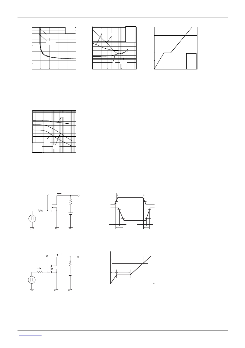
Measurement circuits
V GS
I D
V DS
Pulse Width
D.U.T.
R L
V GS
V DS
50%
10%
10%
90%
50%
10%
R G
V DD
90%
90%
t d(on)
t on
t r
t d(off)
t off
t r
Fig.1-1 Switching Time Measurement Circuit
V G
Fig.1-2 Switching Waveforms
V GS
I D
R L
V DS
V GS
Q g
I G (Const.)
R G
D.U.T.
V DD
Q gs
Q gd
Charge
Fig.2-1 Gate Charge Measurement Circuit
Fig.2-2 Gate Charge Waveform
www.rohm.com
c 2009 ROHM Co., Ltd. All rights reserved.
4/4
2009.06 - Rev.A
发布紧急采购,3分钟左右您将得到回复。
相关PDF资料
RTR030N05TL
MOSFET N-CH 45V 3A TSMT3
RTU002P02T106
MOSFET P-CH 20V 250MA SOT-323
RUE002N02TL
MOSFET N-CH 20V .2A EMT3
RUE003N02TL
MOSFET N-CH 20V 300MA EMT3
RUF015N02TL
MOSFET N-CH 20V 1.5A TUMT3
RUF025N02TL
MOSFET N-CH 20V 2.5A TUMT3
RUL035N02TR
MOSFET N-CH 20V 3.5A TUMT6
RUM002N02T2L
MOSFET N-CH 20V 0.2A VMT3
相关代理商/技术参数
RTR025P02
制造商:ROHM 制造商全称:Rohm 功能描述:Switching (−20V, −2.5A)
RTR025P02TL
功能描述:MOSFET P-CH 20V 2.5A TSMT3 RoHS:否 制造商:STMicroelectronics 晶体管极性:N-Channel 汲极/源极击穿电压:650 V 闸/源击穿电压:25 V 漏极连续电流:130 A 电阻汲极/源极 RDS(导通):0.014 Ohms 配置:Single 最大工作温度: 安装风格:Through Hole 封装 / 箱体:Max247 封装:Tube
RTR030N05
制造商:ROHM 制造商全称:Rohm 功能描述:2.5V Drive Nch MOSFET
RTR030N05TL
功能描述:MOSFET Med Pwr, Sw MOSFET N Chan, 45V, 3A RoHS:否 制造商:STMicroelectronics 晶体管极性:N-Channel 汲极/源极击穿电压:650 V 闸/源击穿电压:25 V 漏极连续电流:130 A 电阻汲极/源极 RDS(导通):0.014 Ohms 配置:Single 最大工作温度: 安装风格:Through Hole 封装 / 箱体:Max247 封装:Tube
RTR030P02
制造商:ROHM 制造商全称:Rohm 功能描述:Switching (-20V, -3.0A)
RTR030P02TL
功能描述:MOSFET P-CH 20V 3A TSMT3 RoHS:否 制造商:STMicroelectronics 晶体管极性:N-Channel 汲极/源极击穿电压:650 V 闸/源击穿电压:25 V 漏极连续电流:130 A 电阻汲极/源极 RDS(导通):0.014 Ohms 配置:Single 最大工作温度: 安装风格:Through Hole 封装 / 箱体:Max247 封装:Tube
RTR040N03
制造商:ROHM Semiconductor 功能描述:MOSFET,Nch,Vdss=30V,Id=4A,TSMT3
RTR040N03_06
制造商:ROHM 制造商全称:Rohm 功能描述:2.5V Drive Nch MOS FET
